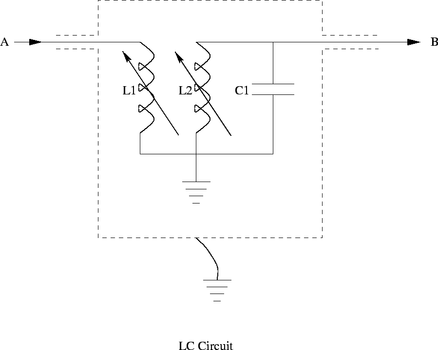
The receiver for the solar flare monitor is a simple circuit designed to detect the 24 KHz signal from the station in Cutler, Maine, and reject signals at nearby frequencies from other directions. The receiver uses a commercial amplified loop antenna manufactured by ``Palomar'' with its ``Omega'' loop. The loop is approximate 25 cm in diameter and can be oriented in any direction. In a concrete and wood building away from significant structural iron the plane of the loop is vertical and its normal is approximately along a line directed from Louisville, KY, to Cutler, ME. This antenna has an internal FET preamp which may be battery operated. In our system the battery is not connected, and the internal circuit has been modified to accept power delivered on the coax from the antenna to the receiver. The amplified RF from the antenna is capacitively coupled to a LC resonator tuned to 24 KHz. This first stage of the receiver is shown in Fig. 1.
 |
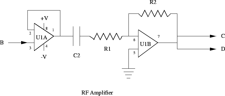
The output from the LC resonator connects to an RF 2-stage amplifier shown
in Fig. 2. The amplifier uses a commonly available LF353
dual JFET opamp with the first stage as a voltage follower of unity
gain, and the second stage with gain
![]() in
this example. The output of this amplifier may be fed directly to
an oscilloscope to monitor tuning of the LC circuit and the antenna.
in
this example. The output of this amplifier may be fed directly to
an oscilloscope to monitor tuning of the LC circuit and the antenna.
 |
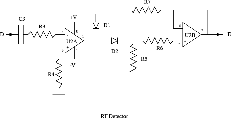
The RF amplifier is capacitively coupled to a detector circuit that rectifies the 24 KHz signal and provides some additional gain. This section also uses an LF353 as shown in Fig. 3.
 |
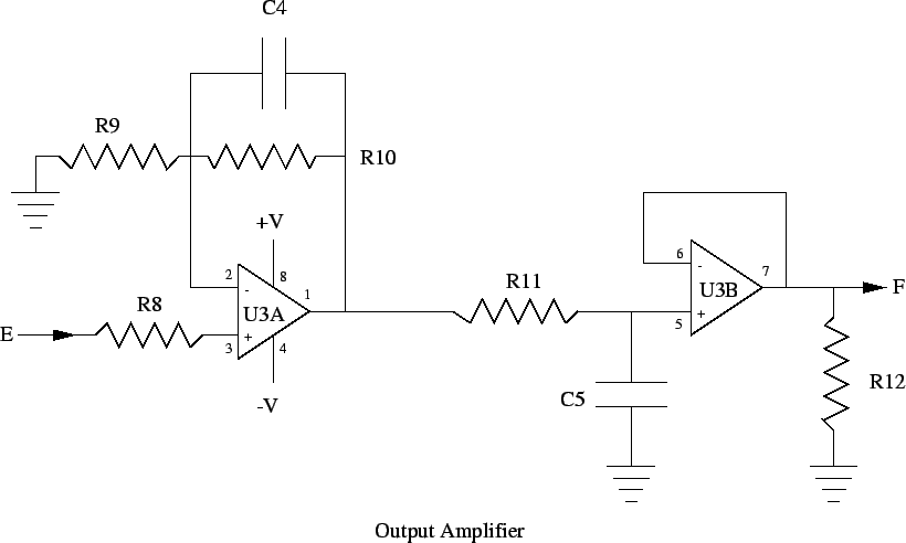
Additional gain, low-pass filtering, and buffering is provided by
a third dual JFET opamp in the section shown in Fig. 4.
The gain is adjusted by the resistor R9, which is omitted for ![]() or decreased to 10K for
or decreased to 10K for ![]() . In this version it is set to
. In this version it is set to ![]() .
The time constant is R11
.
The time constant is R11![]() C5 and is set to 5 s here. The resistor
R12 provides some output loading of the amplifier and is adjusted to minimize
noise. It leads to a BNC jack on the front panel of the amplifier
and a 50
C5 and is set to 5 s here. The resistor
R12 provides some output loading of the amplifier and is adjusted to minimize
noise. It leads to a BNC jack on the front panel of the amplifier
and a 50 ![]() cable connects from there to the analog-to-digital converter
at the computer. An additional RC filter is located at the A-to-D
to properly terminate this cable and minimize noise.
cable connects from there to the analog-to-digital converter
at the computer. An additional RC filter is located at the A-to-D
to properly terminate this cable and minimize noise.
 |